In today’s data centers and clouds, minimizing power consumption is essential.
For example, how important is it to save 25 to 75 watts per server? On an average installation of 24 to 40 servers per rack, it means saving 0.6 to 3.0 kilowatts of power per rack. Now consider that 3 kilowatts are the peak consumption of a single-family home in Europe. Besides, there is the additional cost associated with cooling the heat generated by the power consumed by the server (typically another 60% on top of the energy input cost).
But let’s not get ahead of ourselves, and pause for a moment to analyze why processor power consumption is on the rise.
All modern processors are built using MOSFETs (metal-oxide-semiconductor field-effect transistors). Shrinking the size of these transistors is very desirable because it allows packing more functions on a single chip and reducing the cost and power per feature.
In 1974, Robert Dennard observed that power density remained constant for a given area of silicon (square nanometers) when the dimension of the transistor shrank, thanks to technology improvements (Dennard Scaling).
He observed that voltage and current should be proportional to the linear dimensions of a transistor; thus, as transistors shrank, so did voltage and current. Because power is the product of voltage and current, power dropped with the square. On the other hand, the transistor area fell with the square, and the transistor count increased with the square. The two phenomena compensated each other.
Dennard scaling ended around 2004 because current and voltage couldn’t keep dropping while still maintaining the dependability of integrated circuits, and the leakage current and threshold voltage became the dominant factors in establishing a power baseline per transistor.
With the end of Dennard scaling, with each new transistor generation, power density increased. The following figure gives a qualitative idea of the transistor size and the power (estimated using the International Technology Roadmap for Semiconductors) as a function of the years.
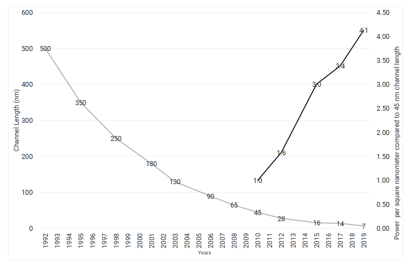
The gray curve is the channel length in nanometers, and the black curve is the power per square nanometer compared to the 45-nanometer channel length.
Moreover, shrinking the size of MOSFET is complicated for various reasons and comes with limitations and reduced benefits:
- Shrinking the size of transistors also implies shrinking the size of the metal traces that interconnect them, and this results in an increased electrical resistance, which, in turn, limits the frequency of operations.
- Reducing the voltage at which circuits operate can be done up to a point. There are minimum threshold voltages, for example, for memory circuits, which cannot be crossed.
- Reducing voltage below a certain level also causes transistors not to switch on and off completely and therefore consume power due to subthreshold conduction.
- There is an intrinsic power dissipation related to distributing the clock along the clock tree, and with more transistors and functions per chip, this clock tree becomes larger.
- Other leakages become important when reducing channel length; for example, gate-oxide leakage and reverse-biased junction leakage. These factors can account for 20% to 50% of the total power consumption of an application-specific integrated circuit (ASIC), depending on the channel length.
Associated with power consumption are heat production and heat dissipation. Maintaining the transistor below a specific temperature is mandatory for device reliability. Economic factors are also important; for example, the adoption of esoteric, expensive technology to cool a chip is usually not practical in commercial systems.
Additionally, the increase in power density poses limitations on:
- Clock frequency, since each bit toggle consumes power, the more frequent changes happen, the more power is consumed.
- Package design, size, and cost, because the current carrying capacity per ball (contact) must increase to keep up with the power density.
As a consequence, it became impossible to continue increasing the performance of a single CPU core by increasing the frequency. Dennard scaling is the dominant factor in the slowdown of the growth of single CPU core performance, i.e., of its SpecINT performance.
With the reduction in transistor channel length, the photolithographic process becomes more critical. It is more difficult to precisely align the fabrication masks and control the dopant numbers and placement. Also, the process requires higher frequencies of light to reduce the wavelength, as the feature size decreases. These factors have significantly increased the cost of manufacturing, and thus the cost of ASICs produced with the 16 and 7nm processes.
Food for thoughts
Given that the growth of a single CPU core is limited by Dennard scaling factor and that we have an established and limited power budget, the question we should ask ourselves is: “Where should we allocate our power budget?”
The typical answer up to now has been: “Allocate as much power as possible to the CPU cores.”
An alternative answer is to allocate some power to hardware optimized for domain-specific processing, i.e., devices specifically designed for a class of workloads, rather than for general-purpose computing. Examples of domain-specific silicon would include GPUs (Graphics Processing Units) or Neural-Network Processors for artificial intelligence and machine learning, as well as networking and security-focused processors.
These alternative processors are more power-efficient than general-purpose processors for the function they perform, i.e., the computational domain they cover.
A solution that uses CPU cores for general-purpose computation and domain-specific hardware for specialized tasks may have a better performance or a lower power consumption compared to a solution that implements everything on CPU cores.